|
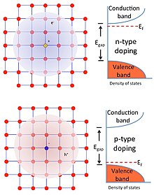
Modulation doping Modulation doping is a technique for fabricating semiconductors such that the free charge carriers are spatially separated from the donors. Because this eliminates scattering from the donors, modulation-doped semiconductors have very high carrier mobilities. HistoryModulation doping was conceived in Bell Labs in 1977 following a conversation between Horst Störmer and Ray Dingle,[1] and implemented shortly afterwards by Arthur Gossard. Störmer and Dan Tsui used a modulation-doped wafer to discover the fractional quantum Hall effect. ImplementationModulation-doped semiconductor crystals are commonly grown by epitaxy to allow successive layers of different semiconductor species to be deposited. One common structure uses a layer of AlGaAs deposited over GaAs, with Si n-type donors in the AlGaAs.[2] ApplicationsField effect transistorsModulation-doped transistors can reach high electrical mobilities and therefore fast operation.[3] A modulation-doped field-effect transistor is known as a MODFET.[4] Low-temperature electronicsOne advantage of modulation doping is that the charge carriers cannot become trapped on the donors even at the lowest temperatures. For this reason, modulation-doped heterostructures allow electronics operating at cryogenic temperatures. Quantum computingModulation-doped two-dimensional electron gases can be gated to create quantum dots. Electrons trapped in these dots can then be operated as quantum bits.[5] References
Information related to Modulation doping |